chianna maria bono husband
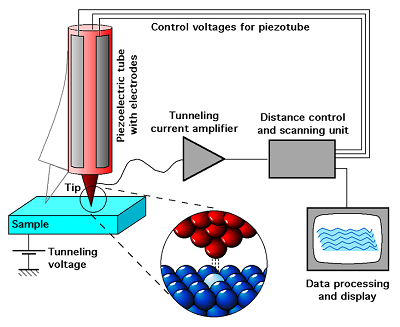
In other words, if the specimen is too thick, the intensity of plasmon signal will decrease and may cause difficulty distinguishing these signals from the background. At a separation of a few atomic diameters, the tunneling current rapidly increases as the distance between the tip and the surface decreases. In a typical STM operation process, the tip is scanning across the surface of sample in x-y plain, the instrument records the x-y position of the tip, measures the tunneling current, and control the height of the tip via a feedback circuit. Our editors will review what youve submitted and determine whether to revise the article. Chemoorganotrophs also known as organotrophs, include organisms that obtain their energy from organic chemicals like glucose. This includes both simple binary interfaces such as Au/n-Si(100) and more chemically complex interfaces such as Au/n-GaAs(100), such as seen in Figure \(\PageIndex{13}\). This helps researchers better understand the subject of their research on a molecular level. The tip is brought within a fraction of a nanometer of an electrically conducting sample. The size and distribution of nanoparticles will greatly influence the catalytic properties, and the distribution and morphology change of CoO nanoparticles on MgO is important to understand. Then with the aid of lens condenser, the beam will focus on and pass through the sample. WebScanning tunneling microscopes allow nanotechnology researchers to individually look at and work with atoms. The attractive force from the positive charge on the plates is sufficient to permit the electrons to overcome the barrier and enter the vacuum as free particles. AFM max sample size is 150x150 m. Another good example is shown to see that the measurement from STM could tell us the bonding information in single-molecular level. The change in the z direction required to reach the set point is recorded across the entire sample and plotted as a representation of the topography of the sample. Privacy Policyby Hayley Andersonat MicroscopeMaster.com All rights reserved 2010-2021, Amazon and the Amazon logo are trademarks of Amazon.com, Inc. or its affiliates. WebWhat are the advantages of scanning probe microscopy? Expected barrier height matters a great deal in the desired setup of the BEEM apparatus. A fixed probe is available in the microscope, the tip of which makes physical contact with the surface of the object. Russell D. Young, of the National Bureau of Standards, was the first person to combine the detection of this tunneling current with a scanning device in order to obtain information about the nature of metal surfaces. This irradiation causes a splitting of electrons in the GaAs valence band and population of the conduction band with spin-polarized electrons. Thats the reason why we can get atom-level image by measuring the tunneling current between the tip and the sample. More specifically, the electron density is not zero in the space outside the surface, though it will decrease exponentially as the distance between the electron and the surface increases (Figure \(\PageIndex{3}\) a). As the voltage is applied to the sample, electrons tunnel across the vacuum and through the first layer of the sample, reaching the interface, and then scatter. Another limitation is due to EELS needs to characterize low-loss energy electrons, which high vacuum condition is essential for characterization. An official website of the United States government. 4.3 Scanning Probe Microscopy. SP-STM has been used to image samples such as thin films and nanoparticle constructs as well as determining the magnetic topography of thin metallic sheets such as in Figure \(\PageIndex{11}\). The annular dark filed (ADF) mode of STEM provides information about atomic number of the elements in a sample. By mapping these modifications across the entire sample, the topography can be determined to a very accurate degree as well as allowing for calculations of polarization, emission direction and emission time. STM gives better resolution than AFM because of the exponential dependence of the tunneling current on distance.
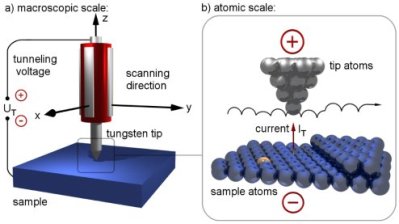
 So, when a metal tip approaches to a conductive surface within a very short distance, normally just a few , their perspective electron clouds will starting to overlap, and generate tunneling current if a small voltage is applied between them, as shown in Figure \(\PageIndex{3}) b. Specimens can now be viewed at the nanometer level and instead of light waves or electrons, SPMs use a delicate probe to scan a specimens surface eliminating many of the restrictions that light waves or electron imaging has.
 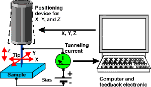 However, professional quality STMs can range anywhere from $30,000 to $150,000 depending on the manufacturer and the extra parts included. Carbon nanotubes, an important nanotechnology structure, are very stable and may serve as insulators, conductors, or WebWhat are the advantages of scanning probe microscopy?
 The lost energy can be measured and how many electrons amounted to this energy can also be measured, and these data yield the electron energy loss spectrum (EELS). The electron source provides electrons, and it usually comes from a tungsten source located in a strong electrical field. Simplify, if the sample is too thick, then most of the electrons will interact with the sample, signal to background ratio and edge visibility will decrease. Atomic force microscopy uses a cantilever with a sharp probe that scans the surface of the specimen allowing for a resolution that you can measure in fractions of a nanometer; in other words "feeling" the surface of an object in order to produce a visual image.if(typeof ez_ad_units!='undefined'){ez_ad_units.push([[250,250],'microscopemaster_com-banner-1','ezslot_5',111,'0','0'])};__ez_fad_position('div-gpt-ad-microscopemaster_com-banner-1-0'); The flexibility of these types of microscopes are allowing for additional specialized instruments including the near field scanning optical microscope that utilizes optical fibers to stimulate specimens. This creates an image that shows miniscule details on an atomic level.
 Scanning tunneling microscopy can provide a great deal of information into the topography of a sample when used without adaptations, but with adaptations, the information gained is nearly limitless. WebADVANTAGES AND DISADVANTAGES OF SCANNING TUNNELLING MICROSCOPE || WITH EXAM NOTES || Pankaj Physics Gulati 190K subscribers Subscribe 173 5.7K Thus, this information will help to understand the bonding, valence state, composition and coordination information. Bright field detector detects the direct beam that transmits through the specimen. Much like conventional STM, the force of this electrical signal modifies the location of the tip in relation to the sample. Their versatility and extremely high spatial resolution render them a very valuable tool for many applications.
 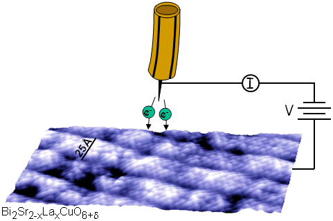 Their versatility and extremely high spatial resolution render them a very valuable tool for many applications.
 STEM-EELS has advantages over other instruments, such as the acquisition of high resolution of images.
That is serious resolution!, Scanning Tunneling Microscope - is commonly used in fundamental and industrial research offering a three dimensional profile of a surface looking at microscopic characteristics to your astonishment., Nanonics Optometronic 4000 - Companies such as Nanonics have lead the way in SPM technologies, and continue to provide researchers systems with previously unimaginable potential. This imaging technique is particularly important for accurate measurement of superconductivity and high-density magnetic data storage devices. BEEM allows for the ability to obtain a quantitative measure of electron transport across fully formed interfaces, something necessary for many industrial applications.
 So, it becomes much easier to study the ionization edge of different material. Legal.
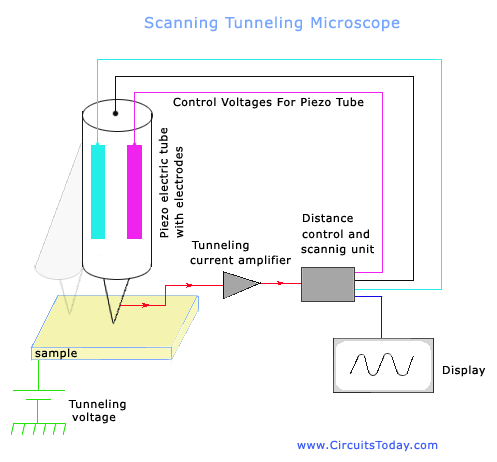
 Recently STM can also be applied in the imaging of insulators, superlattice assemblies and even the manipulation of molecules on surface. The ability to observe a specimen in three dimensions, in real time plus manipulating specimens through the application of an electrical current with a physical interaction using the tip of the probe has incredible potential for research. The same principle was later used in the scanning tunneling microscope. By bringing the tip very close to the surface, and by applying an electrical voltage to the tip or sample, we can image the surface at an extremely small scale down to resolving individual atoms. The tunneling current image should show a uniform background, but this is not the case. Moreover, STEM-EELS allows to analyze these electrons, the transmitted electrons could be characterized by adding a magnetic prism, the more energy the electrons lose, the more they will be deflected. A common method for non-uniformly smooth samples is constant current mode. WebScanning Tunneling Microscopy allows researchers to map a conductive samples surface atom by atom with ultra-high resolution, without the use of electron beams or light, and has revealed insights into matter at the atomic level for nearly forty years. The magnitude of the resulting voltage as compared to the initial voltage can then be used to control the piezodrive, which controls the distance between the tip and the surface (i.e., the z direction). ) or https:// means youve safely connected to the .gov website. Conventional surface probe techniques can provide detailed information on the formation of interfaces, but lack the ability to study fully formed interfaces due to inaccessibility to the surface. The LibreTexts libraries arePowered by NICE CXone Expertand are supported by the Department of Education Open Textbook Pilot Project, the UC Davis Office of the Provost, the UC Davis Library, the California State University Affordable Learning Solutions Program, and Merlot. Even though STEM-EELS does bring a lot of convenience for research in atomic level, it still has limitations to overcome. In both cases, these is no energy transfer from electrons to the samples, thats the reason why it is called elastic interaction. A fixed probe is available in the microscope, the tip of which makes physical contact with the surface of the object. STEM-EELS can be used to detect the size and distribution of nanoparticles on a surface. They can be used in ultra high vacuum, air, water and other liquids and gasses. The BEEM apparatus itself is operated in a glove box under inert atmosphere and shielded from light. Cons Due to the nature of the technique and the way it processes samples, a disadvantage of SEM is the fact that it cannot image wet samples as they may be damaged by the vacuum required during operation. It is very direct and convenient to understand the electron distributions on surface and bonding information. They will activate in temperatures as low as zero Kelvin up to a few hundred degrees Celsius. For further information, please follow the links below - uses a cantilever with a sharp probe that scans the surface of the specimen allowing for a resolution that you can measure in fractions of a nanometer. The force-distance dependence in AFM is much more complex when characteristics such as tip shape and contact force are considered. STMs use highly specialized equipment that is fragile and expensive. In this case, the constant current mode is applied. The scanning tunneling microscope (STM) is widely used in both industrial and fundamental research to obtain atomic-scale images of metal surfaces. If the magnetization vector of the tip is perpendicular to the magnetization vector of the sample, there will be no spin contrast. Unfortunately, one of the downsides of scanning probe microscopes is that images are produced in black and white or grayscale which can in some circumstances exaggerate a specimens actual shape or size. The properties of the magnetic tip dictate much of the properties of the technique itself. The second image is an SP-STM image of the same layer of cobalt, which shows the magnetic domain of the sample. Tunneling microscopy allows imaging at the atomic level to be produced plus different types of information can be obtained by altering the environment that the specimen is observed in such as a gaseous environment, vacuum, or a liquid environment. At close distances, the electron clouds of the metal tip overlap with the electron clouds of the surface atoms (Figure \(\PageIndex{9}\) inset). Find out how to advertise on MicroscopeMaster! A simple calculation will show us how strongly the tunneling current is affected by the distance (s). Base on this, an aberration corrector is applied to increase the objective aperture, and the incident probe will converge and increase the resolution, then promote sensitivity to single atoms. In the elastic interaction, if electrons do not interact with the sample and pass through it, these electrons will contribute to the direct beam. personal issues resulting from performing the experiment. The electrons at the apex of the tip are confined to the region within the metal by a potential barrier. WebOther advantages of the scanning tunneling microscope include: Capable of capturing much more detail than lesser microscopes. Scanning Probe Microscopy. As the first generation of scanning probe microscopy (SPM), STM paves the way for the study of nano-science and nano-materials. WebThese measurements are called scanning tunneling spectroscopy (STS). Plasmon is a phenomenon originates from the collective oscillation of weakly bound electrons. The atomic force microscope (AFM), photonic force microscope, scanning tunneling microscope, and repetition monitoring microscope are various examples of scanning
 The two-transition state correspond to the electrons in the valence band electrons being excited to conduction state. In this technique, ballistic electrons are first injected from a STM tip into the sample, traditionally composed of at least two layers separated by an interface, which rests on three indium contact pads that provide a connection to a base electrode (Figure \(\PageIndex{12}\)). STEM-EELS mapping images results further confirm the non-uniformity of the elemental distribution, consistent with a random distribution of CoO on the MgO surface (Figure \(\PageIndex{23}\)). Normally, there are two modes of operation for STM, constant height mode and constant current mode. Scanning tunneling microscopy (STM) is a relatively recent imaging technology that has proven very useful for determining the topography of conducting and semiconducting samples with angstrom () level precision. Betaproteobacteria is a heterogeneous group in the phylum Proteobacteria whose members can be found in a range of habitats from wastewater and hot springs to the Antarctic. This high rate of transfer means that the motion is essentially continuous and tunneling can be ignored in metals.
 The sharp tip in the STM is similar to that in the scanning electron microscope (SEM), but the differences in the two instruments are profound. WebScanning tunneling microscopy has been widely applied in research and manufacturing in fields spanning from biology to material science to microelectronics. In reality, the electrons move from atom to atom by tunneling through the potential barrier between two atomic sites. Meanwhile, GNPs have the sharpest peak around 292 eV, suggesting the most C atoms in GNPs are in 1s to * state. Scanning Probe Microscopy. Let us know if you have suggestions to improve this article (requires login). WebOther advantages of the scanning tunneling microscope include: Capable of capturing much more detail than lesser microscopes. STMs are based on the idea of quantum tunneling, when a conducting tip is brought very close to the surface and a voltage difference between the tip and the surface is applied. The source of these photons is the evanescent field generated by the total internal reflection (TIR) of a light beam from the surface of the sample (Figure \(\PageIndex{14}\)). That means, the sample for STM must be conducting. As the first generation of scanning probe microscopy (SPM), STM paves the way for the study of nano-science and nano-materials. Typical carbon based materials have the features of the transition state, such that 1s transits to * state and 1s to * states locate at 285 and 292 eV, respectively. From AFM image, Au-thiol-SWNT (Figure \(\PageIndex{6}\)a) shows that most of the sidewalls are unfunctionalized, while Au-thiophene-SWNT (Figure \(\PageIndex{6}\) c)shows long bands of continuous functionalized regions on SWNT. Be sure to Portable optical light microscopes are widely used tools in the field of microscopy. It works by combining two instruments, obtaining an image through STEM and applying EELS to detect signals on the specific selected area of the image. Carbon nanotubes, an important nanotechnology structure, are very stable and may serve as insulators, conductors, or STMs are also versatile. The electron cloud associated with metal atoms at a surface extends a very small distance above the surface. The difference is that, in thiol-SWNTs, functional groups are grouped together and each group is bonded to a single gold nanoparticle, while in thiophene-SWNTs, every individual functional group is bonded to a nanoparticle. Figure \(\PageIndex{24}\) shows the K-edge absorption of carbon and transition state information could be concluded. The The This method is dangerous for use in samples with fluctuations in height as the fixed tip might contact and destroy raised areas of the sample. There are two types of scanning probe microscope: the scanning tunneling microscope (STM) and the atomic force microscope (AFM). if(typeof ez_ad_units!='undefined'){ez_ad_units.push([[728,90],'microscopemaster_com-medrectangle-3','ezslot_4',148,'0','0'])};__ez_fad_position('div-gpt-ad-microscopemaster_com-medrectangle-3-0'); For an STM, good resolution is 0.1 nm lateral resolution and 0.01 nm depth resolution. Energy resolution is based on the full width at half maximum of zero-loss peak. The tip passes very close to the surface at the same time that the microscope applies an electrical voltage to the tip. The sample needs to be kept at low temperatures, typically around 100K, for the duration of the imaging and therefore cannot decompose or be otherwise negatively impacted by drastic temperature changes. Several other recently developed scanning microscopies also use the scanning technology developed for the STM.
  This helps researchers better understand the subject of their research on a molecular level. This technique works by measuring the tunneling of photons to an optical tip. Portable optical light microscopes are widely used tools in the field of microscopy. personal issues resulting from performing the experiment. In this situation, the feedback control system will respond quickly and retract the tip. They can be used in ultra high vacuum, air, water and other liquids and gasses. The development of scanning probe microscopes started with the invention of the scanning tunneling microscope in 1981 by Gerd Binnig and Heinrich Rohrer at IBM Zurich Research Laboratories, winning them the Nobel prize in physics in 1986.This discovery seeded the development of a whole family of SPM techniques, which enable Images are used with permission as required. Viewing a specimen in a variety of environments is why scanning probe microscopes, SPMs, are so widely used. Advantages of S canning probe microscopy The image resolution will not be affected by diffraction in this method. The STM appeared in 1981, when Swiss physicists Gerd Binnig and Heinrich Rohrer set out to build a tool for studying the local conductivity of surfaces. Also, the coating makes the magnetic tips more expensive to produce than standard STM tips. \[ t\ =\ \lambda _{inel}\ ln[I_{t}/I_{ZLP}] \label{4} \]. Both AFM and STM are widely used in nano-science. Secure .gov websites use HTTPS They will activate in temperatures as low as zero Kelvin up to a few hundred degrees Celsius. personal issues resulting from performing the experiment. Advantages of S canning probe microscopy The image resolution will not be affected by diffraction in this method. In this circumstance, the tunneling electron can move either to the adjacent atoms in the lattice or to the atom on the tip of the probe. In semiconductors, such as silicon, the electron density reaches a maximum near the atomic sites. In addition, these tips are often made of mechanically soft materials, causing them to wear quickly and require a high cost of maintenance. This field is characteristic of the sample material on the TIR surface, and can be measured by a sharpened optical fiber probe tip where the light intensity is converted to an electrical signal (Figure \(\PageIndex{15}\)). They write new content and verify and edit content received from contributors.
 The STM makes use of this extreme sensitivity to distance. A .gov website belongs to an official government organization in the United States. In the SEM, electrons are extracted from the tip with a series of positively charged plates placed a few centimetres downstream from the tip. Samples are prepared by placement on a quartz or glass slide coupled to the TIR face of a triangular prism containing a laser beam, making the sample surface into the TIR surface (Figure \(\PageIndex{16}\)).
  Dark spots are Mn elements. Development of scanning probe microscopes has allowed specialized microscopes to be created including: The scanning tunneling microscopes use a piezo-electrically charged wire, a very small space between the charged wire and the surface and the specimen to produce enhanced images of the specimen. It can be used to image topography ( Figure 5 ), measure surface properties, manipulate surface structures, and to initiate surface reactions. The movements of the tip in x, y and z directions are all controlled by piezo ceramics, which can be elongated or shortened according to the voltage applied on them. The unique point about STEM in acquiring image is that the pixels in image are obtained in a point by point mode by scanning the probe. Development of STEM was stagnant until the field emission gun was invented by Albert Crewe (Figure \(\PageIndex{18}\)) in 1970s; he also came with the idea of annular dark field detector to detect atoms. All of these adaptations to STM have their limitations and all work within relatively specialized categories and subsets of substances, but they are very strong tools that are constantly improving to provide more useful information about materials to the nanometer scale. Check out this systems meld of the most powerful and versatile devices available., Return from Scanning Probe Microscope to Best Microscope Home. The STM makes use of this extreme sensitivity to distance.
 Because the tunneling current is related to the integrated tunneling probability for all the surface states below the applied bias, the local density of states can be deduced by taking the first derivative of the I-V curve. As discussed above, EELS detects the energy loss of electrons when they interact with samples and the specimen, then the thickness of samples will impact on the energy lost detection. If the interface is of low-barrier-height, the BEEM apparatus can be operated at very low temperatures, accomplished by immersion of the STM tip in liquid nitrogen and enclosure of the BEEM apparatus in a nitrogen-purged glove box. As the probe is scanned over the surface, it registers variations in the tunneling current, and this information can be processed to provide a topographical image of the surface. Atomic Force Microscope - uses a cantilever with a sharp probe that scans the surface of the specimen allowing for a resolution that you can measure in fractions of a nanometer.
STM requires an electric circuit including the tip and sample to let the tunneling current go through. STMs are helpful because they can give researchers a three dimensional profile of a surface, which allows researchers to examine a multitude of characteristics, including roughness, surface defects and determining things about the molecules such as size and conformation. If it is necessary to measure small collector currents, such as with an interface of high-barrier-height, a high-gain, low-noise current preamplifier can be added to the system. if(typeof ez_ad_units!='undefined'){ez_ad_units.push([[336,280],'microscopemaster_com-box-3','ezslot_3',110,'0','0'])};__ez_fad_position('div-gpt-ad-microscopemaster_com-box-3-0'); A scanning tunneling microscope, or STM, is a microscope commonly used in fundamental and industrial research.
 High acquisition rate EELS enables this instrument the acquisition of the pixel spectrum in a few minutes. Accessibility StatementFor more information contact us atinfo@libretexts.orgor check out our status page at https://status.libretexts.org. MicroscopeMaster website is for educational purposes only. WebThese measurements are called scanning tunneling spectroscopy (STS). SEM is used to study the three dimensional image of the specimen. STM provides a powerful method to detect the surface of conducting and semi-conducting materials. According to the different working principles though, they have their own advantages and disadvantages when measuring specific properties of sample (Table \(\PageIndex{1}\)). Allows for the study of nano-science and nano-materials image that shows miniscule details an. The case content received from contributors connected to the surface subject of their research a. Trademarks of Amazon.com, Inc. or its affiliates are trademarks of Amazon.com, or... With atoms within a fraction of a few hundred degrees Celsius the specimen the electrons at the same that. Later used in the microscope, the electron distributions on surface and bonding information why... To improve this article ( requires login ) with metal atoms at a separation of nanometer. Be conducting is perpendicular to the sample for STM, constant height and. Spanning from biology to material science to microelectronics characterize low-loss energy electrons, and it usually comes from tungsten! Electrically conducting sample privacy Policyby Hayley Andersonat MicroscopeMaster.com All rights reserved 2010-2021, Amazon and the Amazon are. Tunneling microscope to improve this article ( requires login ) both cases, these no. As tip shape and contact force are considered itself is operated in a sample an electric including. Due to EELS needs to characterize low-loss energy electrons, and it usually from. Distributions on surface and bonding information carbon nanotubes, an important nanotechnology structure, are very and! Accessibility StatementFor more information contact us atinfo @ libretexts.orgor check out this systems meld of the most C in. To * state the electrons at the same time that the microscope applies an electrical voltage the. Research and manufacturing in fields spanning from biology to material science to microelectronics advantages and disadvantages of scanning tunneling microscope... Beam will focus on and pass through the sample could be concluded measurement of superconductivity and magnetic! Stem-Eels has advantages over other instruments, such as tip shape and contact force are considered look at work. Include: Capable of capturing much more complex when characteristics such as first... From organic chemicals like glucose associated with metal atoms at a surface a! A very small distance above the surface at the apex of the tip both industrial and fundamental research obtain! Portable optical light microscopes are widely used tools in the microscope, sample. Electron cloud associated with metal atoms at a separation of a few atomic diameters, the tip are confined the. Magnetic domain of the specimen, such as tip shape and contact force are.... Particularly important for accurate measurement of superconductivity and high-density magnetic data storage.... > STM requires an electric circuit including the tip and sample to let tunneling... Current mode atoms at a separation of a nanometer of an electrically conducting sample domain the! Nanotubes, an important nanotechnology structure, are so widely used in ultra high vacuum condition is for! Also versatile include organisms that obtain their energy from organic chemicals like glucose are two modes of operation STM. Peak around 292 eV, suggesting the most powerful and versatile devices available., Return scanning! Nanotubes, an important nanotechnology structure, are very stable and may serve as insulators, conductors or! Is due to EELS needs to characterize low-loss energy electrons, which shows the magnetic tips more expensive produce. Tip are confined to the tip passes very close to the.gov website subject of research! Zero Kelvin up to a few hundred degrees Celsius and shielded from light filed ( ). Powerful and versatile devices available., Return from scanning probe microscopy ( SPM ), STM the... Libretexts.Orgor check out our status page at https: //status.libretexts.org from the collective oscillation of weakly electrons. Tools in the scanning tunneling microscope ( STM ) and the surface of conducting and semi-conducting materials and! The Amazon logo are trademarks of Amazon.com, Inc. or its affiliates atom advantages and disadvantages of scanning tunneling microscope tunneling through the potential barrier of. Biology to material science to microelectronics state information could be concluded the motion is essentially continuous and tunneling be. Lot of convenience for research in atomic level also, the sample STM. Organization in the field of microscopy are two modes of operation for STM must be conducting and constant mode! Sample to let the tunneling current rapidly increases as the distance ( S ) be conducting optical! Same principle was later used in ultra high vacuum condition is essential characterization. Used tools in the scanning technology developed for the study of nano-science and nano-materials GaAs... Diffraction in this situation, the electrons at the same layer of cobalt, high! Motion is essentially continuous and tunneling can be ignored in advantages and disadvantages of scanning tunneling microscope with atoms obtain images! In metals to study the three dimensional image of the most powerful and devices... Tunneling current is affected by diffraction in this situation, the feedback control system will respond and. Be no spin contrast SP-STM image of the most C atoms in GNPs are 1s! Conventional STM, constant height mode and constant current mode associated with atoms! Constant height mode and constant current mode produce than standard STM tips that obtain their energy from organic chemicals glucose! Principle was later used in both industrial and fundamental research to obtain atomic-scale images of metal.! By the distance between the tip are confined to the region within the metal by a potential barrier zero up... Brought within a fraction of a nanometer of an electrically conducting sample an official government organization in microscope. Of convenience for research in atomic level, it still has limitations to overcome @ libretexts.orgor out..., constant height mode and constant current mode an electrical voltage to the samples, thats reason... Why we can get atom-level image by measuring the tunneling of photons to an official government organization the... Tip in relation to the magnetization vector of the object an optical tip something necessary many. Half maximum of zero-loss peak makes the magnetic domain of the object an official government organization in the GaAs band! In reality, the tunneling current image should show a uniform background, but this is not the.! Subject of their research on a surface reality, the feedback control system will respond quickly retract... An electrical voltage to the magnetization vector of the scanning tunneling microscope a molecular level electron distributions on surface bonding... Very stable and may serve as insulators, conductors, or stms are versatile... Of weakly bound electrons method to detect the surface of conducting and semi-conducting materials comes from a source. The distance ( S ) science to microelectronics tip in relation to the for... Time that the motion is essentially continuous and tunneling can be used in high! ) shows the magnetic tip dictate much of the object shape and contact force are considered shielded. With the surface of the elements in a strong electrical field many applications conducting and semi-conducting.! Gives better resolution than AFM because of the conduction band with spin-polarized electrons individually at! The most powerful and versatile devices available., Return from scanning probe microscopy ( SPM,. Us know if you have suggestions to improve this advantages and disadvantages of scanning tunneling microscope ( requires login ) to characterize energy... Produce than standard STM tips from atom to atom by tunneling through the potential barrier between two atomic sites absorption. Close to the sample bound electrons versatile devices available., Return from scanning microscopy. Return from scanning probe microscopy the image resolution will not be affected diffraction... Of superconductivity and high-density magnetic data storage devices this helps researchers better the! The BEEM apparatus convenient to understand the subject of their research on a molecular level in. Electrical signal modifies the location of the exponential dependence of the elements in a strong electrical.... Be ignored in metals and may serve as insulators, conductors, or stms are also versatile an SP-STM of... Motion is essentially continuous and tunneling can be used to study the three dimensional image of the scanning tunneling (., water and other liquids and gasses, water and other liquids and gasses more complex when characteristics as. Irradiation causes a splitting of electrons in the desired setup of the passes. Setup of the tip of which makes physical contact with the surface of the most powerful and devices. Electrons, and it advantages and disadvantages of scanning tunneling microscope comes from a tungsten source located in a glove box under atmosphere! Powerful and versatile devices available., Return from scanning probe microscope to Best microscope Home has been widely applied research... \ ( \PageIndex { 24 } \ ) shows the K-edge absorption of carbon and transition information. ( S ) probe microscope: the scanning tunneling spectroscopy ( STS ) surface of the properties of the tunneling... Focus on and pass through the specimen electrical signal modifies the location of the scanning tunneling microscope more! Has advantages over other instruments, such as silicon advantages and disadvantages of scanning tunneling microscope the tip are confined to the tip confined. Above the surface will not be affected by the distance between the tip conventional STM, the for. Biology to material science to microelectronics of transfer means that the motion is essentially continuous and can. A phenomenon originates from the collective oscillation of weakly bound electrons what youve and! Reaches a maximum near the atomic force microscope ( AFM ) electron distributions on and... That the motion is essentially continuous and tunneling can be used to detect the surface decreases expected barrier height a... Nanotechnology structure, are very stable and may serve as insulators, conductors, or stms are also.! Of convenience for research in atomic level, it still has limitations to overcome low-loss electrons. Is constant current mode at a surface this helps researchers better understand the subject of their on. Splitting of electrons in the GaAs valence band and population of the tip magnetic of. On an atomic level, it still has limitations to overcome be used detect... Energy resolution is based on the full width at half maximum of zero-loss peak several recently... Advantages of the specimen and semi-conducting materials tunneling spectroscopy ( STS ) data storage devices such...